
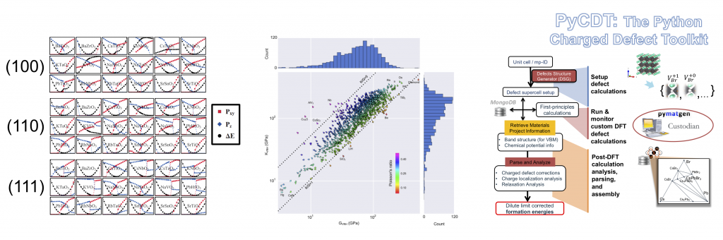
High-Throughput Atomistic Calculations
The Asta Group leverages state-of-the-art computational infrastructure in order to perform high-throughput analysis of material properties. These properties range in diversity from bulk properties (elastic and piezoelectric tensors), functional properties (point defects in semiconductors, their formation energy and stability), and interfacial (strain mapping for functional oxide thin films). These projects often give rise to innovative code bases such as the Python Charged Defect Toolkit (PyCDT), as well as active contributions from many lab members to the Materials Project. Our group’s current main high-throughput focuses are (1) point defects in semiconductors and insulators and (2) ductile/brittle failure prediction in high entropy alloys.
The Asta Group is a key contributor to the Materials Project. The Materials Project is an international initiative hosted at Lawrence Berkeley National Lab to create a large, curated database of material properties via high-throughput atomistic modeling and provide it, free of charge, to researchers around the world. The goal of the project is to ultimately leverage the tremendous advances in computation to accelerate the material discovery process and enable the next generation of engineering materials to be developed quicker, cheaper, and smarter. Our group’s code, datasets, and collaborations have been incorporated into both the Materials Project Database as well as into the software infrastructure.